“Surface modification of hard diamond particles with Cu–Mo₂C double layer coating and its application in thermal conductive composites
October16, 2025
As the power density and integration level of semiconductor chips continue to increase, thermal management materials for electronic packaging are required to exhibit both high thermal conductivity and a low coefficient of thermal expansion (CTE). Traditional composites such as W–Cu and SiC–Cu suffer from high density and limited thermal conductivity, making them inadequate for high heat flux applications.
Diamond, with its ultrahigh thermal conductivity (1200–2000 W/m·K) and extremely low CTE, is considered an ideal thermal reinforcement phase. However, its poor interfacial wettability and high thermal boundary resistance with copper have severely restricted the performance of diamond/copper composites.
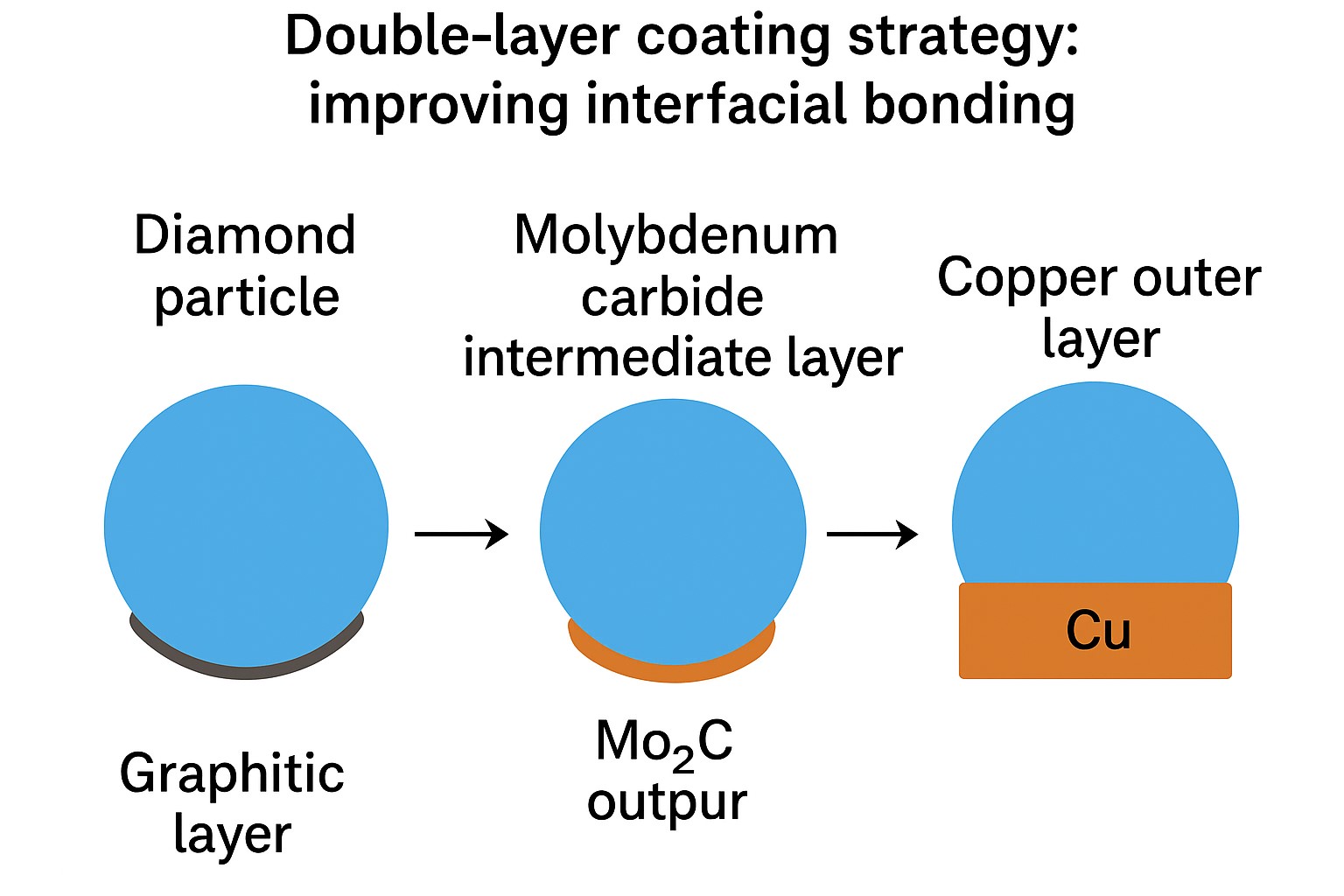
Double-layer coating strategy: improving interfacial bonding
To address this issue, a research team from the University of Science and Technology Beijing proposed a copper–molybdenum carbide (Cu–Mo₂C) double-layer coating approach. The related study, titled “Surface modification of hard diamond particles with Cu–Mo₂C double layer coating and its application in thermal conductive composites”, was published in Diamond & Related Materials.
In this work, the researchers first employed a molten-salt method at 1000 °C, where molybdenum trioxide (MoO₃) reacted with the graphitized layer on the diamond surface to form a stable Mo₂C interlayer. This layer significantly enhances the chemical compatibility between diamond and copper. Subsequently, a pure copper outer layer was deposited onto the Mo₂C-coated diamond via electroless plating. The resulting Cu–Mo₂C double-layer structure improves interfacial wettability and promotes strong bonding between diamond particles and the copper matrix.
This approach offers a cost-effective and practical route for fabricating diamond/copper composites. The Cu–Mo₂C coating enables uniform dispersion of diamond particles at high volume fractions (up to 70 vol%) while achieving excellent thermal conductivity and thermal compatibility. The process is simple, does not require high-pressure or complex infiltration equipment, and shows great potential for applications in chip packaging substrates, high-power electronic devices, and data center thermal management.
The study demonstrates both theoretically and experimentally that this dual-layer interface design effectively enhances interfacial bonding and thermal performance, providing valuable insights for the development of other high-performance metal matrix composites.


