
Diamond Semiconductor Materials: Progress, Challenges and Future Directions
September27, 2026
Diamond Semiconductor Materials: Progress, Challenges and Future Directions
Diamond is increasingly regarded as one of the most promising materials for next-generation semiconductor technologies. As a representative fourth-generation semiconductor, diamond combines an ultra-wide bandgap, extremely high thermal conductivity, high breakdown electric field, high carrier mobility, and excellent chemical stability. These properties make it particularly attractive for high-power, high-frequency, high-temperature, radiation-resistant, and extreme-environment electronics. The reviewed literature identifies diamond as a potential platform for advanced power electronics, RF and microwave systems, quantum technologies, high-performance sensors, and other applications where conventional semiconductor materials face fundamental thermal or electrical limitations.
The development of practical diamond semiconductor devices, however, depends on more than the intrinsic properties of diamond. Three material and process challenges remain particularly important: producing large-area, low-defect single-crystal diamond substrates; achieving controllable and efficient n-type doping; and developing thermally and chemically stable surface and interface structures.
1. High-Quality Single-Crystal Diamond Substrates
The quality of the diamond substrate directly determines the performance and reliability of subsequent semiconductor structures. Key parameters include crystal size, orientation, impurity concentration, dislocation density, surface quality, and thickness.
Two major technologies dominate the development of semiconductor-grade single-crystal diamond: high-pressure high-temperature (HPHT) synthesis and chemical vapor deposition (CVD).
HPHT diamond is produced under pressures of approximately 5–6 GPa and temperatures of roughly 1,300–2,300 °C using metallic catalysts. High-quality HPHT type-IIa diamond can achieve very low impurity concentrations and low defect densities, making it an excellent seed material for CVD epitaxy. Its principal limitation for semiconductor applications is size. Nevertheless, its high crystal quality makes HPHT diamond particularly valuable as a substrate for subsequent epitaxial growth.
CVD, particularly microwave plasma CVD (MPCVD), provides greater flexibility in controlling growth conditions, impurity concentration, crystal orientation, thickness, and doping. Advances in MPCVD equipment and reactor design have enabled the growth of increasingly large single-crystal diamond, with reported dimensions reaching the centimeter scale and beyond. High-purity CVD diamond can achieve extremely low impurity concentrations and low dislocation densities, making it suitable for high-end semiconductor, quantum, optical, and epitaxial applications.
The combination of the two technologies is therefore particularly important: high-quality HPHT diamond can serve as the seed substrate, while CVD provides scalable epitaxial growth. This hybrid strategy offers a pathway toward larger and higher-quality semiconductor-grade diamond substrates.
Other approaches, including hot-filament CVD, detonation synthesis, solution growth, heteroepitaxy, and interface-induced growth, provide alternative routes for diamond films, composite structures, nanocrystalline materials, or potentially large-area growth. However, the review indicates that HPHT and MPCVD remain the principal technologies for high-end single-crystal semiconductor applications.
2. P-Type Diamond: A Relatively Mature Direction
Compared with n-type diamond, p-type diamond is considerably easier to realize. Boron (B) is currently the dominant p-type dopant because the atomic radius of boron is close to that of carbon. The relatively small atomic-size mismatch allows boron to substitute for carbon in the diamond lattice.
Boron introduces an acceptor level approximately 0.37 eV above the valence band. This enables the generation of holes and p-type electrical conduction. By controlling the boron concentration, growth conditions, defect density, and activation behavior, researchers can tailor the electrical properties of p-type diamond.
B-doped diamond has already been investigated in a range of device structures, including Schottky barrier diodes, field-effect transistors, UV photodetectors, electrochemical electrodes, microwave devices, and various sensors. Its combination of high thermal conductivity, wide bandgap, high breakdown capability, and chemical stability makes it particularly attractive for high-temperature and high-power applications.
Nevertheless, p-type diamond is not yet a completely solved technology. Excessive boron concentration can introduce defects, impurity clustering, lattice stress, and reduced carrier mobility. Achieving uniform doping, high activation efficiency, low defect density, and stable interfaces remains important for improving device consistency and scalability.
3. N-Type Diamond: The Critical Bottleneck
The development of high-quality n-type diamond remains one of the most difficult problems in diamond semiconductor technology.
The fundamental challenge arises from the mismatch between potential donor atoms and the carbon lattice. While the atomic-radius difference between boron and carbon is only about 6.5%, potential n-type dopants such as phosphorus, sulfur, and arsenic have substantially larger atomic-radius differences. This makes substitutional incorporation into the diamond lattice difficult and can generate significant lattice damage and defects.
Phosphorus is currently regarded as one of the most promising n-type dopants. However, phosphorus introduces a relatively deep donor level of approximately 0.57 eV. As a result, although very high phosphorus concentrations can be incorporated into diamond, only a small fraction of the dopants may contribute free electrons at room temperature. Reported activation rates for conventional P-doped diamond can therefore remain extremely low.
This creates a fundamental distinction between dopant concentration and electrically active carrier concentration. Increasing the total phosphorus concentration alone does not necessarily produce useful n-type conductivity. Dopant incorporation, lattice damage, activation energy, carrier mobility, and defect compensation must all be addressed simultaneously.
One particularly interesting direction described in the review is ultra-high-pressure thermal diffusion. A 15 GPa HPHT diffusion process was proposed to reduce the effective atomic-size mismatch between phosphorus and carbon under extreme pressure. The reported material achieved a phosphorus concentration of approximately 10²⁰ cm⁻³, a room-temperature electron concentration of approximately 10¹⁸ cm⁻³, and a resistivity of about 2 Ω·cm.
However, this approach also revealed significant limitations. The resulting carrier mobility was only approximately 2.78 cm²/(V·s), partly associated with the extremely high dopant concentration and surface degradation. Thus, high-pressure processing provides an important proof of concept for efficient n-type activation, but further optimization is required to simultaneously achieve high carrier concentration, high mobility, low defect density, and good surface quality.
CVD-based phosphorus doping has also demonstrated promising results, including high-quality n-type epitaxial layers and n-type MOSFET structures. Such results indicate that controlled epitaxial growth and device engineering may provide another route toward practical n-type diamond electronics. Nevertheless, the narrow process window, slow growth rate, strict equipment requirements, and high manufacturing cost remain challenges for large-area production.
Multi-element approaches such as P-S, P-N, and P-B co-doping are also being explored. The objective is to modify the electronic structure, reduce impurity clustering and compensation, and potentially shallow the donor level. At present, however, these approaches remain largely at the research and development stage.
4. Hydrogen-Terminated Diamond and Two-Dimensional Hole Gas
Surface termination provides another important method for controlling diamond's electronic properties.
Hydrogen termination changes the surface electronic structure of diamond and can induce a two-dimensional hole gas (2DHG). Through charge transfer involving the hydrogen-terminated surface and surrounding polar species, the diamond surface can exhibit high-mobility p-type conductivity without conventional bulk elemental doping.
Hydrogen-terminated diamond has therefore attracted considerable attention for field-effect transistors, high-frequency electronics, high-temperature devices, chemical sensors, biological sensors, and microfluidic systems.
The technology also offers significant flexibility in device engineering. Hydrogen plasma treatment can create the conductive surface, while dielectric and gate-stack engineering can be used to control the channel and improve device characteristics. High-k dielectric materials such as Al₂O₃ and ZrO₂ have been investigated for interface engineering and transistor optimization.
The major limitation is stability. Surface conductivity depends strongly on the surface condition and surrounding environment. Long-term reliability, interface control, metallization, environmental compatibility, and reproducibility across large areas remain important engineering challenges.
5. Oxygen-Terminated Diamond and Interface Engineering
Oxygen termination provides a different approach to controlling diamond surfaces. Chemical or plasma treatment introduces oxygen-containing functional groups such as C=O and C–OH, modifying surface states, band bending, work function, and interface properties.
Compared with hydrogen termination, oxygen termination is generally associated with reduced surface conductivity but improved surface passivation and chemical stability. This makes oxygen-terminated diamond particularly relevant to dielectric integration, metal contacts, sensors, and other structures where stable interfaces are more important than highly conductive surfaces.
The review emphasizes that surface termination should therefore be considered not simply as a method of controlling conductivity, but as a broader interface-engineering technology. Future work will need to address the behavior of terminated surfaces under high temperature, strong electric fields, radiation, and other extreme operating conditions.
6. From Materials Science to Diamond Semiconductor Technology
The progress of diamond semiconductor technology is ultimately determined by the ability to integrate high-quality materials into reproducible devices.
At the substrate level, the industry needs larger, cleaner, lower-defect single-crystal diamond at lower cost. At the doping level, p-type diamond is relatively established, while efficient and high-mobility n-type diamond remains a critical bottleneck. At the surface and interface level, hydrogen and oxygen termination provide powerful tools for electronic control, but their thermal, chemical, and radiation stability must be improved.
These challenges are closely interconnected. A high-quality substrate is required for low-defect epitaxy; controlled doping is required for functional p-n junctions and complementary device structures; and stable interfaces are essential for reliable MOSFETs, Schottky diodes, sensors, and integrated circuits.
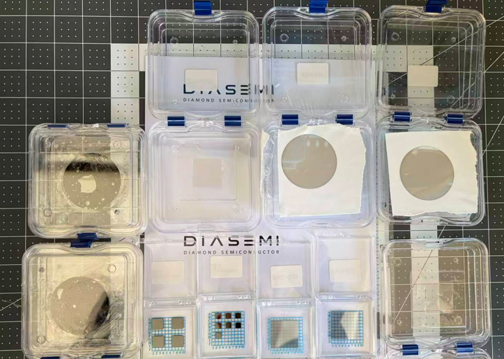
The review therefore points toward an integrated development strategy combining HPHT seed technology, advanced MPCVD epitaxy, controlled elemental doping, ultra-high-pressure processing, surface termination, interface engineering, and advanced device fabrication.
7. Outlook
Diamond possesses an unusual combination of electrical, thermal, mechanical, and chemical properties that could enable semiconductor devices operating beyond the practical limits of many conventional materials. Its potential is particularly significant in high-power electronics, RF and microwave systems, quantum information, high-temperature electronics, radiation-resistant systems, and high-performance sensing.
However, diamond semiconductor technology is still constrained by materials cost, substrate size, defect control, doping efficiency, device processing, and long-term reliability. Among these challenges, efficient n-type diamond and scalable semiconductor-grade substrates are particularly critical.
Future progress will depend on simultaneously improving crystal size and quality, reducing manufacturing cost, increasing dopant activation, controlling defects and interfaces, and developing stable device architectures. The combination of HPHT and MPCVD provides a promising substrate strategy, while advanced high-pressure doping and surface/interface engineering may open new routes toward functional diamond electronics.
The transition from laboratory demonstrations to industrial semiconductor platforms will therefore require not one single breakthrough, but the coordinated development of diamond crystal growth, doping, surface chemistry, metallization, device fabrication, packaging, and reliability engineering. As these technologies mature, diamond could become an important material platform for the next generation of high-power, high-frequency, high-temperature, and extreme-environment semiconductor systems.